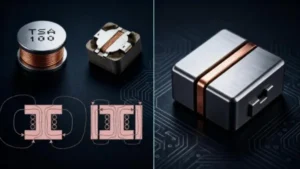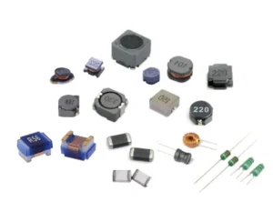
Four main types of surface-mount inductors exist: wire-wound, multilayer, braided, and thin-film. The two most common are wire-wound and multilayer. The former is a miniaturized version of the traditional wire-wound inductor; the latter is produced using multilayer printing and manufacturing technologies, offering a smaller footprint than wire-wound chip inductors and representing a key product in the field of inductive components.
Commonly used surface-mount chip inductors fall primarily into two categories: wire-wound and multilayer. The former are miniaturized versions of traditional wire-wound inductors, whereas the latter are manufactured using multilayer printing and lamination processes; multilayer chip inductors are more compact than their wire-wound counterparts and represent a key area of development in the field of inductive components.
(★ If you want to know more information, you can refer to the following article: •2026 Inductor Industry: 3 Key Trends)


1. Wire-Wound Inductors
These inductors are characterized by a wide inductance range (from millihenries to henries), high inductance precision, low loss (i.e., high Q-factor), high current-carrying capacity, mature manufacturing processes, simple construction, and low cost; however, they face limitations in further miniaturization. Ceramic-core wire-wound chip inductors maintain stable inductance values and relatively high Q-factors at extremely high frequencies, making them significant components in high-frequency circuits.
TDK’s NL series inductors are wire-wound components offering inductance values ranging from 0.01 to 100 µH with a 5% tolerance; featuring high Q values, they meet the requirements of standard applications.
The NLC type is suitable for power supply circuits and supports rated currents up to 300 mA; the NLV type offers high Q values and an eco-friendly design (utilizing recycled plastic) while remaining compatible with the NL series; the NLFC type features magnetic shielding and is suitable for power lines.
Typical applications include power supply circuits, DC-DC converters, energy storage, filtering, and resonant circuits, spanning sectors such as telecommunications, automotive electronics, and consumer electronics (e.g., mobile phones, computers, and routers).
2. Multilayer Chip Inductors
These inductors feature excellent magnetic shielding, high sintering density, and robust mechanical strength. Their drawbacks include lower production yields, higher costs, and relatively low inductance and Q values. Compared to wire-wound chip inductors, they offer numerous advantages: compact dimensions that facilitate circuit miniaturization; a closed magnetic circuit design that prevents interference with or from surrounding components, enabling high-density component mounting; an integrated structure ensuring high reliability; excellent heat resistance and solderability; and a uniform shape suitable for automated Surface Mount Technology (SMT) production.
TDK’s MLK series inductors are characterized by their compact size, solderability, and magnetic shielding, utilizing a high-density integrated design to ensure high reliability. The MLG series employs high-frequency ceramic materials and offers lower inductance values, making it suitable for high-frequency circuits; the MLK series supports operating frequencies up to 12 GHz and features high Q values alongside low inductance values (1 nH–22 nH).
Typical applications: Power management and signal filtering in portable electronic devices such as mobile phones, laptops, tablets, digital cameras, and Bluetooth headsets.
3. Thin-Film Chip Inductors
These components feature high Q-factors, high precision, high stability, and compact dimensions—characteristics that are maintained even in the microwave frequency range. Due to the coplanar arrangement of internal electrodes and the concentrated magnetic field distribution, the device’s parameters remain stable after mounting, and it exhibits excellent frequency characteristics at frequencies above 100 MHz.
Typical applications: RF circuits and microwave-range applications, such as high-frequency signal processing in 5G communications and Wi-Fi modules.
4. Woven-style inductor
Key features include: higher inductance per unit volume at 1 MHz compared to other chip inductors, compact size, and ease of mounting on substrates. They can serve as miniature magnetic components in power-handling applications. In practical applications, selection should be based on specific requirements, with a balanced consideration of performance and cost.
Typical applications: Scenarios requiring miniature magnetic components for power handling.

Wire-wound chip inductors are primarily used in power supply circuits (particularly for DC-DC conversion) and high-frequency circuits, with widespread applications in consumer electronics, automotive electronics, and communication equipment. They are widely adopted for their high current-handling capability, broad inductance range, high Q values, low losses, and robust, reliable structure.
Key Application Scenarios
1. Power Supply Circuits: This is a primary application area. They are used in switching power supplies and DC-DC converters to perform functions such as energy storage, filtering, current limiting, and voltage regulation—for example, in power modules for mobile phones and routers.
2. Filtering and Noise Suppression: Used for EMI (Electromagnetic Interference) filtering and noise suppression to mitigate interference on power and signal lines and improve signal quality.
3. RF (Radio Frequency) Circuits: Used in RF chokes, LC matching networks, and tuning circuits. Wire-wound inductors with ceramic cores feature high self-resonant frequencies, making them ideal for high-frequency applications such as mobile phone RF modules and wireless communication equipment.
4. Consumer Electronics: Widely used in devices such as mobile phones, laptops, tablets, TWS (True Wireless Stereo) earbuds, and smartwatches.
5. Automotive Electronics: Applied in areas such as new energy battery systems, in-vehicle electronic equipment, and motor control.
Typical Application Example
Taking TWS (True Wireless Stereo) earbuds as an example: The MWPH/MWPU series of wire-wound chip power inductors from Sunlord Electronics is specifically designed for such wearable devices.
Background noise suppression: Featuring a magnetically shielded structure, these inductors minimize magnetic flux leakage and reduce interference with surrounding components, thereby lowering background noise in TWS earbuds.
Extended battery life: Optimized core materials and winding processes reduce both DC resistance (DCR) and AC resistance (ACR), minimizing power loss and extending battery life.
Miniaturization: Available in various sizes ranging from 1.0 × 0.5 mm to 1.6 × 0.8 mm, meeting the miniaturization requirements of wearable devices.
Key Factors For Component Selection:
Distinguish between application scenarios: For power circuits requiring high current and high inductance values, wire-wound inductors are the first choice; while multilayer inductors, due to their small footprint, are suitable for extreme miniaturization and high-density mounting, but their power handling capacity is relatively low.
Consider high-frequency characteristics: Wire-wound inductors exhibit parasitic capacitance effects at high frequencies and have a limited self-resonant frequency (SRF); the actual operating frequency must remain well below the SRF to avoid capacitive behavior.
Pay attention to magnetic shielding performance: Traditional open magnetic circuit wire-wound inductors may generate electromagnetic interference (EMI); therefore, for magnetically sensitive designs, products with magnetic shielding should be given priority.
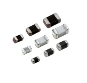
Multilayer chip inductors are primarily used in high-frequency circuits to perform functions such as filtering, resonance, impedance matching, and choking. Their features include small size, excellent magnetic shielding performance, and suitability for high-density surface mounting, making them widely used in major fields such as consumer electronics, communications, automotive electronics, and industrial automation.
Consumer Electronics Applications
Typical Applications: Noise suppression for input/output lines and DC-DC conversion circuits in devices such as smartphones, laptops, digital cameras, and hard disk drives.
Fast Charging: With the adoption rate of smartphone fast-charging technology exceeding 90%, multilayer inductors—thanks to their compact size and high energy efficiency—have become the standard choice for fast-charging circuits in smartphones and laptops.
Advantages: Compact dimensions and a closed magnetic circuit design prevent interference with surrounding components, making them ideal for high-density circuit board mounting.
Communications Applications
RF Front-End: Multilayer ceramic inductors are the mainstream choice for RF applications, serving functions such as coupling, resonance, and choking in RF communications; there is significant demand for miniaturized (e.g., 0201 size) LTCC multilayer high-frequency inductors in 5G RF front-end systems.
Wireless Modules: Multilayer chip high-frequency inductors are utilized in the matching circuits of components such as mobile phone RF modules, Wi-Fi modules, and Bluetooth modules.
5G Base Stations: Thanks to their cost-effectiveness, 0402-size products have achieved a market penetration rate exceeding 70% in base station filter circuits.
Automotive Electronics Applications
Powertrain and Control Systems: Suitable for automotive powertrain systems; automotive-grade products cover systems such as battery management, ADAS, and in-vehicle infotainment.
Reliability and Temperature: Automotive-grade multilayer inductors feature a wide operating temperature range (e.g., -55°C to +155°C) and meet the environmental and vibration requirements of autonomous driving; hundreds of units may be used in a single vehicle.
Application Scenarios: Automotive multimedia, wireless connectivity, and body and comfort systems.
Industrial and Other Applications
Industrial Automation: Used for current control and EMI suppression to enhance equipment immunity to interference.
Power Management: Multilayer power inductors are suitable for switching power supply circuits operating in the megahertz range with high switching frequencies, offering inductance values up to several microhenries (µH).
Office Equipment and Home Appliances: Noise suppression on input/output lines for products such as digital televisions, video recorders, and personal computers.
Selection Guide for Multilayer Chip Inductors
For high-frequency circuits, priority should be given to self-resonant frequency and Q-factor; for power management circuits, rated current and DC resistance are the primary considerations. If miniaturization is required, small-sized packages such as 0603 or 0805 may be considered. Multilayer inductors generally have lower rated currents and inductance values; wire-wound inductors are typically better suited for high-power applications or scenarios requiring high inductance values.
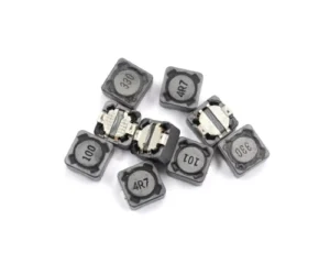
Woven-type chip inductors are compact and offer high inductance per unit volume, serving primarily as miniature magnetic components for power handling.
Characteristics of Braided Chip Inductors.
1. Core advantages: Compared to other chip inductors, it has a higher inductance per unit volume at 1 MHz; its compact size facilitates mounting on a substrate.
2. Typical applications: Used as miniature magnetic components for power handling; ideally suited for applications requiring compact dimensions and high power density.
3. Comparison: Unlike multilayer inductors, which feature a closed magnetic circuit and strong anti-interference capabilities, wound-type inductors do not have a fully closed magnetic circuit; however, they exhibit lower magnetic leakage in high-frequency applications.
Braided chip inductors are mainly used in miniaturized circuits related to power processing. Considering the overall application scenarios of chip inductors, common application areas include:
1. Automotive electronics: Used in power modules such as motor controllers, DC-DC converters, and on-board chargers to smooth pulse current and stabilize output.
2. Smart Devices and Consumer Electronics: Power management and signal filtering for portable devices such as mobile phones, laptops, and digital cameras.
3. Industrial Control: Energy storage and filtering in power modules and power conversion circuits, meeting the requirements for high-density assembly.
4. Communication Equipment: Noise suppression and impedance matching in RF modules and power supply lines.
Selection Guide for Wire-Wound Chip Inductors
Wire-wound inductors offer advantages in terms of compact size and inductance density; however, if magnetic shielding (to prevent interference with surrounding components) or suitability for high-density automated assembly is the priority, multilayer inductors may be more appropriate. Conversely, if the application requires high current capacity, high precision, and low loss, wire-wound inductors offer superior performance. Final selection should take into account factors such as operating frequency, rated current, and available circuit board space.
Key characteristics of thin-film chip inductors include compact size, high precision, and excellent high-frequency performance; consequently, they are primarily used in applications with stringent space and frequency requirements, such as mobile phones and wireless communications.
Key Application Areas
1. Mobile Phones and Consumer Electronics: Used in RF modules, power amplifiers, and power management circuits within smartphones, facilitating miniaturization and high-density integration.
2. Wireless Communication: Maintains high Q-factors and stability in the microwave frequency range (above 100 MHz), making it ideal for high-frequency signal processing circuits.
3. Automotive Electronics: Used for power filtering in modules such as ADAS cameras and automotive radar; requires high-temperature resistance (125–150°C) and high reliability.
4. On-Chip Power Delivery (IVR): A cutting-edge application involving the integration of inductors directly into the chip package to power CPUs and GPUs. Apple’s M-series chips and Intel’s Xeon processors utilize similar solutions to replace traditional external inductors.
How to Choose Based on the Application Scenario?
Scenario 1: RF front-end / Mobile phones.
Key requirements: High Q-factor, high precision, compact size.
Suitable type: Standard thin-film chip inductors.
Scenario 2: Integrated Voltage Regulators (IVR) on-chip.
Key requirements: Ultra-thin profile, nanosecond-level response, compatibility with chip fabrication processes.
Suitable types: Magnetic-clad RDL inductors / Nano-laminated inductors.
Scenario 3: High-current power delivery (e.g., AI chips).
Key requirements: High saturation current, low DCR.
Suitable type: Vertical structure solutions (e.g., Intel Coax MIL).
When Purchasing Thin-Film Chip Inductors, Pay Attention to These Points:
Inductance range: typically between 0.6nH and 100nH, with inductance accuracy of ±1%~2%.
Q-factor and Self-Resonant Frequency (SRF): For high-frequency applications, prioritize the Q-factor (ideally >15 at 100 MHz) and SRF (ideally >400 MHz).
Current capability: Calculate the circuit’s peak current first, then verify that the inductor’s saturation current (Isat) provides sufficient margin.
Temperature range: Automotive-grade products must support a range of -40°C to 125°C or even higher.
Key Selection Criteria for Common SMD Wire-Wound Inductors
Prioritize wire-wound types for power applications: Wire-wound inductors are more suitable for scenarios requiring high current and high inductance, such as power converters and energy storage circuits, whereas multilayer types have lower current-handling capabilities.
Consider materials and manufacturing processes for high-frequency applications: Ceramic-core wire-wound inductors are suitable for GHz-range RF applications; Ni-Zn ferrite types are suitable for the tens-to-hundreds of MHz range; and thin-film types offer higher high-frequency Q-factors and tighter tolerances.